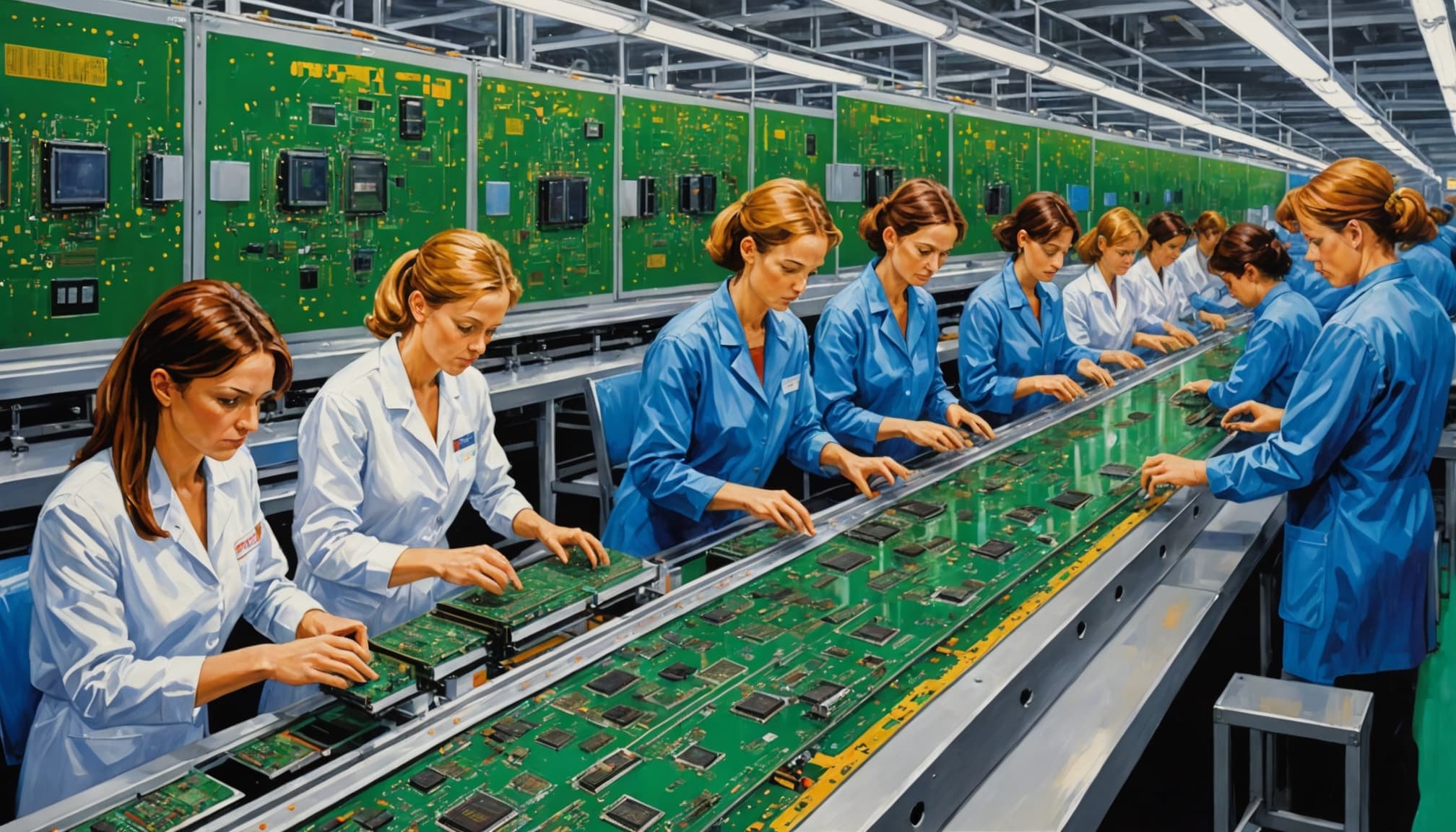
Odisha has signed a historic Memorandum of Understanding with Intel and 3D Glass Solutions of the US for the establishment of India's first-of-its-kind Advanced Packaging Substrate Manufacturing Facility. The tripartite agreement was signed in New Delhi in the presence of Anu Garg, chief secretary of Odisha; Vishal Kumar Dev, additional chief secretary, Electronics and IT, Odisha; and Lip-Bu Tan, Intel chief executive officer. Odisha Chief Minister Mohan Charan Majhi and Union Minister for Electronics and IT Ashwini Vaishnaw joined virtually. The project will establish an advanced semiconductor packaging and glass-core substrate manufacturing facility in the Bhubaneswar-Khordha region over the next five to six years, with the facility expected to be implemented in phases to bring in foreign direct investment of nearly $3.3 billion. As reported by Business Standard, the facility will manufacture advanced packaging glass-core substrates and high-density interconnect substrates, which are critical components used in advanced chip packaging technologies.
The proposed facility will manufacture advanced packaging glass-core semiconductor substrates and high-density interconnect substrates, which are critical components used in advanced chip packaging technologies. As reported by official statements, the facility will leverage advanced glass-based substrate technologies and high-density interconnect packaging, essential for sectors such as AI, high-performance computing, telecommunications, and next-generation electronics. Intel will serve as the technology partner, providing process expertise, technology licensing, quality systems, and workforce capability-building support. The project will house world-class cleanrooms, fabrication units, testing infrastructure, and research and development facilities. According to Business Standard, Babu Mandava, CEO of 3D Glass Solutions, said the proposed project has the potential to establish India as a key global hub for advanced glass substrates and semiconductor packaging, supporting high-growth sectors such as artificial intelligence, high-performance computing and next-generation electronics. Naga Chandrasekaran, executive vice-president and general manager of Intel Foundry, said the collaboration will help explore new opportunities in Odisha and accelerate the commercialisation of next-generation advanced packaging solutions globally.
The project is expected to generate nearly 1,800 direct high-skilled jobs, along with a significant number of indirect employment opportunities. According to official statements, the initiative will directly contribute to Odisha's ambitious target of becoming a $500 billion economy by 2036 and a $1.5 trillion economy by 2047. The project will also promote a transition towards high-quality, knowledge-based employment generation, which has been identified as a key pillar under Odisha's 'Vision 2036' roadmap. Additionally, the facility is expected to enhance GST collections and increase state revenues through manufacturing activities, ancillary industries, and supply chain development, thereby strengthening Odisha's long-term tax base and export earnings. As reported by Business Standard, Chief Minister Majhi emphasized that the glass substrate initiative goes beyond semiconductor manufacturing, creating a future where Odisha becomes a globally competitive destination for advanced technologies, innovation, AI infrastructure, data centres and digital transformation.
The project will facilitate the development of a comprehensive semiconductor ecosystem in Odisha, including advanced materials, specialty chemicals, glass substrates, capital equipment manufacturing in the upstream sector, electronics manufacturing, system integration, and export-oriented industries in downstream sectors. According to Business Standard, officials said the project can trigger the emergence of a broader semiconductor ecosystem comprising upstream suppliers of speciality chemicals, advanced materials, capital equipment and glass substrates, as well as downstream electronics and system integration industries. The initiative will drive cluster-based industrialisation by attracting global players and accelerate Odisha's transformation into a semiconductor manufacturing hub. The ambitious initiative will position Odisha as a centre for niche semiconductor technologies, including advanced packaging and materials engineering. The project is also expected to strengthen academia-industry partnerships and boost research and development, innovation, and skill development ecosystems in the state, creating a future-ready talent pipeline aligned with global semiconductor industry demands.
Minister Vaishnaw highlighted that the entry of firms like Applied Materials Inc, Lam Research, Tokyo Electron Ltd, Merck Electronics, and the signing of the MoU between Tata Electronics and Dutch multinational ASML represents recognition of the government's efforts in the semiconductor sector and industry trust in India. As reported by Business Standard, Chief Minister Majhi stated that their vision is to build a vibrant ecosystem that creates world-class opportunities, attracts leading global technology companies and firmly places Odisha on the global semiconductor map, besides strengthening India's technological self-reliance. The $3.3 billion investment represents one of the largest high-technology manufacturing investments in the country and marks the first project with the engagement of computer chip major Intel in India's semiconductor manufacturing landscape. According to Business Standard, Niti Aayog's report emphasizes that India must be among the top three destinations for OSAT and advanced packaging to compete in the global semiconductor market.