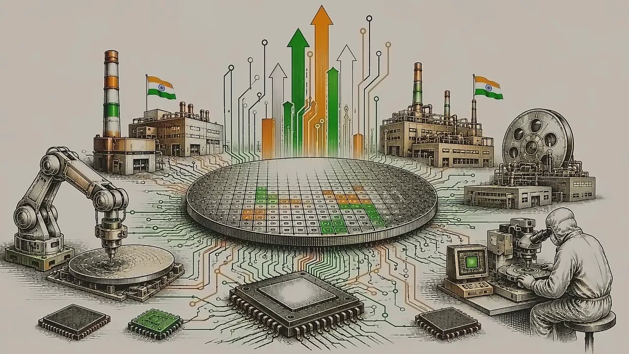
India is in the final stages of preparing Semicon 2.0, the next phase of its semiconductor mission, with the government set to broaden incentives beyond chip fabrication to support the country's wider semiconductor ecosystem. As per The Times of India, ISM CEO Amitesh Kumar Sinha confirmed during an online session on Monday that the policy is being finalised and will be announced soon. The revised programme will "broaden the eligibility criteria and improve the incentive structure" for semiconductor design startups, marking a significant expansion from the previous focus on manufacturing facilities.
Under ISM 2.0, the government plans to provide fiscal support of up to 50% for multiple semiconductor segments including silicon fabrication units, compound semiconductor facilities, assembly and testing units, and chip design. According to NDTV Profit, the proposed scheme places greater emphasis on financial and non-financial incentives for compound semiconductor units and manufacturers of gases, ingots and other raw materials used in chip fabrication and packaging. The mission aims to strengthen semiconductor manufacturing, chip design, and skill development, while positioning the sector as a key driver of economic resilience, digital infrastructure, and technological self-reliance.
Unlike the first phase, which focused primarily on attracting fabrication and packaging investments, Semicon 2.0 aims to strengthen every layer of the chip value chain. As reported by The Times of India, the revised programme will expand support beyond fabs to include chip design startups as well as suppliers of semiconductor-grade chemicals, gases, materials and manufacturing equipment. This comprehensive approach reflects the government's push to build a complete domestic chip ecosystem rather than focusing only on manufacturing facilities. The mission will also scale talent development initiatives and indigenous research in critical semiconductor technologies, ensuring a holistic approach to semiconductor development.
The approved projects show a clear focus on assembly and packaging capabilities, with majority being assembly, testing, marking and packaging (ATMP) units, as well as outsourced assembly, testing and packaging (OSAT) facilities. As reported by Business Standard, this composition reflects the government's strategy to establish comprehensive semiconductor manufacturing infrastructure across multiple stages of the value chain. Among the approved projects, India's first display fabrication unit and the first chip fabrication unit are particularly noteworthy developments, with the chip fabrication facility being established by the Tata Group. These facilities are strategically located across Gujarat, Uttar Pradesh, Assam, Andhra Pradesh, Odisha, and Rajasthan.
The approval of these 12 semiconductor projects represents a substantial investment in India's electronics manufacturing ecosystem and positions the country as a serious player in the global semiconductor supply chain. As reported by NDTV Profit, as of 31 December 2025, the government had approved 10 major semiconductor projects with cumulative investments of around ₹1.60 trillion across six Indian states. The enhanced support is expected to accelerate project execution, attract greater private investment, and expand domestic capacity across the semiconductor value chain. The proposed ISM 2.0 outlay represents the next phase of India's semiconductor programme, with a broader incentive framework aimed at strengthening manufacturing, design capabilities and the domestic semiconductor supply chain.