China remains approximately 15 years behind in developing cutting-edge chipmaking tools, according to UBS analysts led by Francois-Xavier Bouvignies. In a new report, UBS stated that China appears to be at a stage similar to ASML in 2004, when the Dutch company was developing its EUV lithography technology. The analyst team cited patent activity centered on light sources and laser subsystems, noting that China's technology shows a level of maturity comparable to ASML 15 years before it began mass-producing EUV machines. This assessment aligns with earlier estimates from UBS analysts who wrote this week that China is likely at least a decade away from developing domestic EUV technology. The executive emphasized that "it doesn't really come as a surprise and now we need to see how capable these tools really are," adding that "we are still way ahead."
The technology gap comes as the US maintains export controls on advanced semiconductor equipment. The US bars ASML Holding NV, a Zeiss shareholder, from shipping its most advanced machines to China, while Beijing continues investing in domestic semiconductor development. According to Bloomberg reports, any expansion of export controls to include legacy DUV machines would negatively impact business, as Rohmund stated the company "doesn't believe in the positive impact of these export restrictions because it accelerates innovation in China." The US also requires export licenses for several of ASML's more sophisticated immersion DUV models, with China being one of ASML's top markets for previous generation DUV technology. UBS expects that "given the likely gap in yield and throughput versus ASML and the regulatory constraints, Chinese-made lithography tools are unlikely to be used outside China," adding that "uncertainty remains because information on the tools' performance and the capabilities of China's semiconductor supply chain is limited."
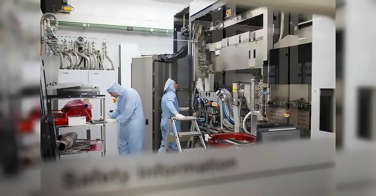
Despite years of development efforts, none of China-based makers of lithography have established mass production of immersion DUV scanners capable of producing chips at 45nm and below. However, recent developments show significant progress in domestic manufacturing capabilities. According to Reuters reports, China has begun mass-producing domestically developed immersion deep-ultraviolet (DUV) lithography machines, with Shanghai Aishengna Electronic Technology Group leading the production effort. The company has brought in teams from several leading domestic lithography startups and is reportedly manufacturing equipment capable of making chips on nodes down to 28nm. UBS expects China to gain the ability to mass-produce immersion DUV lithography machines within two to five years, though these machines still cannot match EUV in drawing the finest circuit patterns. The complexity of photolithography, which requires tens of thousands of individual components with extraordinary positional accuracy, has proven challenging for Chinese manufacturers to replicate.
While China shows progress in DUV technology, its EUV development remains significantly behind international standards. A late-2025 Reuters investigation revealed that China had moved beyond the research stage to a EUV prototype completed in early 2025, which was undergoing testing and reportedly occupies nearly an entire factory floor. According to people familiar with the project, the system is operational and can generate EUV light, but has yet to produce a working chip. UBS reports that China is unlikely to develop EUV tools within the next decade, with the technology gap remaining substantial. The scale of China's EUV ambitions is reflected in Beijing's pursuit of a secretive, state-backed effort to build a homegrown EUV lithography system, likened to China's "Manhattan Project" due to the vast resources behind the initiative.
Despite export restrictions, ASML's China business continues to face challenges as Beijing's push for semiconductor self-sufficiency weighs on demand. China accounted for 14% of ASML's net system sales by shipment location in Q2 2026, down from 19% in Q1, according to the company's latest results. However, China's semiconductor investment boom is creating significant opportunities for domestic equipment suppliers. Goldman Sachs forecasts that wafer-fab equipment spending in China will rise from roughly US$44.3 billion this year to US$53 billion in 2027 and US$60.7 billion in 2028. This spending surge is particularly benefiting local equipment suppliers, particularly in the memory sector, with NAND giant YMTC moving toward fabs built predominantly with domestically sourced tools.