Indian semiconductor startups are achieving significant milestones despite commercial challenges. According to reports from Mint, Mindgrove Technologies successfully exited the lab in June 2025, securing an alliance with Prama India to integrate its homegrown vision system-on-chip into CCTV cameras. The breakthrough was facilitated by India's April 2024 policy change requiring disclosure of chip origins and banning non-certified imported cameras from April 2026. However, the MoU with Prama India is not an immediate commercial order, with prototypes expected by end-2025 and commercial orders contingent on product qualification.
The commercial timeline for fabless startups reveals significant challenges. As reported by Mint, BigEndian's camera silicon prototype, developed since September 2024, is expected to be ready around November 2025, with revenue generation potentially starting April 2027 - approximately three years after chip development began. The startup faces substantial cost disadvantages, with IP licensing costs of about $5 million for Indian companies compared to less than $2 million for Chinese competitors. Indian startups also face longer lead times, with BigEndian's prototype delivery delayed from four months to nearly seven months.
India's semiconductor mission has provided substantial support infrastructure. According to Mint, the India Semiconductor Mission launched in 2021 is backed by a ₹76,000 crore framework covering manufacturing, packaging, testing and chip design, supporting 24 design projects and providing access to tools for 105 startups. The India Semiconductor Mission 2.0 approved in July 2025 expands the budget to ₹1.27 trillion and focuses on chip design, equipment, materials, fabrication, R&D and talent development. About 12 manufacturing projects worth more than ₹1.64 trillion have been approved, with three companies in commercial production. As of June 2026, India had 12 semiconductor manufacturing projects approved with an investment pipeline of approximately USD 17.18 billion, comprising one semiconductor fabrication unit, two compound-semiconductor fabrication units, and nine semiconductor packaging units.
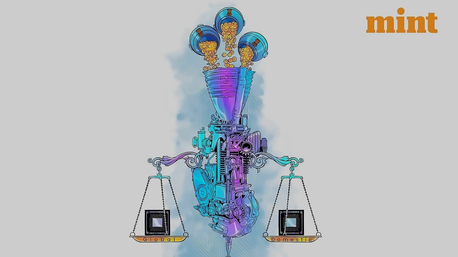
Indian startups face significant competitive disadvantages in the global semiconductor market. As reported by Mint, Indian startups ordering 1,000 wafers monthly cannot command the same capacity and mindshare from foundries as companies ordering 100,000 wafers. The global EDA market is dominated by Synopsys, Cadence and Siemens EDA, whose commercial tool suites can run into millions of dollars. Component costs can increase from budgeted $1.80 to actual $8 due to currency depreciation, logistics, insurance and other costs. Industry leaders acknowledge that Indian companies are at a disadvantage, with the government exploring aggregate demand from multiple Indian companies to secure better foundry terms. However, recent developments show progress, with DLI-supported Vervesemi Microelectronics raising USD 10 million in February 2026 to develop chips for BLDC fans and EVs.
Despite policy support, Indian chip startups face fundamental challenges in achieving commercial viability. According to Mint, MeitY Secretary S. Krishnan emphasizes that Indian chips ultimately must compete globally and cannot depend permanently on government support. The government plans to support companies developing EDA tools, with fabs that establish EDA flows required to use them once developed. Industry experts note that each month is expensive for startups, with delays proving costly for companies like BigEndian that must wait three years for meaningful revenue generation. The CCTV policy experience provides a potential model for similar approaches in smart meters, IoT devices, and e-passports. Looking ahead, India's semiconductor market is projected to grow from USD 54 billion in 2025 to USD 92 billion by 2032, representing a CAGR of around 7.69% during the forecast period, as the country moves from being primarily a design and consumption hub toward manufacturing and supply-chain destination.