India is stepping up its domestic semiconductor manufacturing push with the Centre planning to disburse ₹7,100 crore in incentives this fiscal year under a fresh set of project targets. According to two government officials aware of the development, the funding is expected to attract approximately ₹15,000 crore in fresh investment and generate around 4,700 jobs. The government expects this comprehensive approach to strengthen domestic semiconductor manufacturing and design capabilities across the value chain.
Under the fiscal year 2027 plan, the department of expenditure has tasked the ministry of electronics and information technology with supporting one semiconductor fabrication unit and nine semiconductor manufacturing facilities. The semiconductor fab unit will receive ₹2,000 crore in fiscal support and is expected to attract ₹4,000 crore in investments while generating employment for 1,500 people. The nine units under the scheme for compound semiconductors, silicon photonics, sensors, discrete semiconductor fabs and semiconductor assembly, testing, marking and packaging facilities will receive ₹5,000 crore in fiscal support and are expected to attract around ₹11,000 crore in investments, generating employment for about 3,000 people.
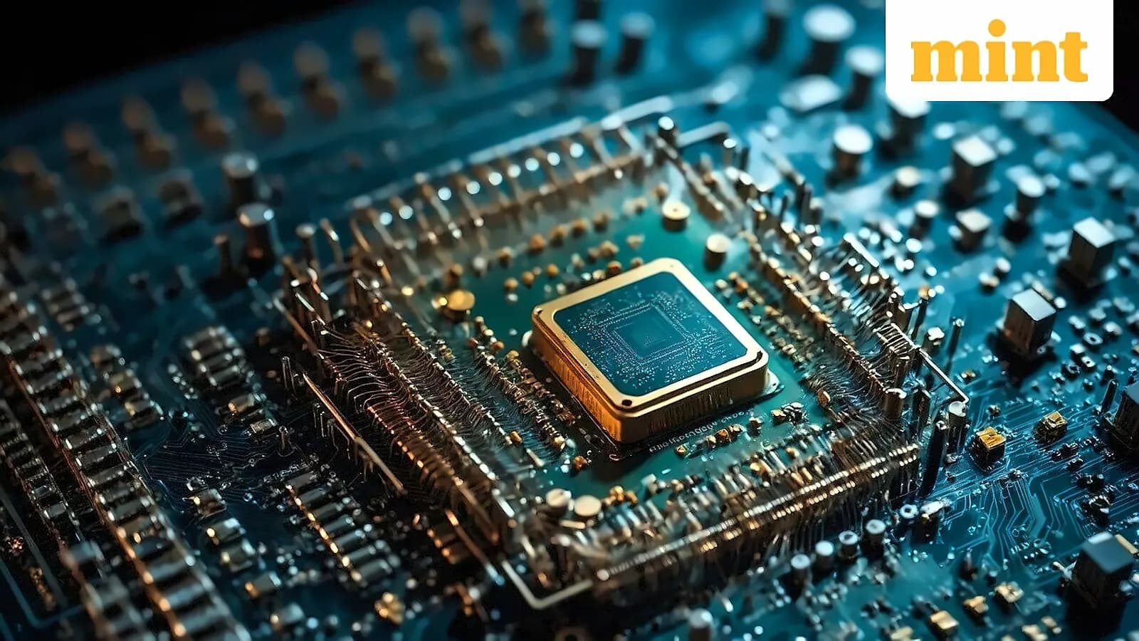
Separately, under the Design Linked Incentive scheme, MeitY will support 30 semiconductor design companies with ₹100 crore to develop 10 semiconductor intellectual property cores and employ 200 design professionals. As reported by government officials, the DoE has allocated ₹7,100 crore for incentive disbursal in FY27 under the programme, with the clear objective of strengthening domestic semiconductor manufacturing and design capabilities. Targeted incentive disbursal in the previous fiscal was about ₹4,000 crore, with actual disbursal figures yet to be released.
India launched a ₹76,000 crore semiconductor mission in December 2021 to develop a domestic semiconductor and display manufacturing ecosystem and reduce dependence on imports in critical technologies. The dozen projects approved under the India Semiconductor Mission include Tata Electronics' semiconductor fabrication facility at Dholera in Gujarat, being set up in partnership with Taiwan's Powerchip Semiconductor Manufacturing Corp. (PSMC). Other approved projects include Micron Technology's assembly, testing, marking and packaging facility and CG Semi's outsourced Osat facility at Sanand, as well as Tata Electronics' assembly and test facility at Jagiroad in Assam. In May this year, the Union cabinet approved two additional semiconductor projects in Gujarat, including an integrated compound semiconductor fabrication and ATMP facility by Crystal Matrix Ltd and an Osat facility by Suchi Semicon Pvt. Ltd.
Industry experts said the government's approach reflects a push to build capabilities across the semiconductor value chain rather than focus solely on manufacturing. Ajai Chowdhry, founder of HCL, said the direction looks promising, noting that it is critical for India to build domestic semiconductor manufacturing capacity. He emphasized that the focus on supporting 30 design companies is very positive, as India's strength lies in chip design with a large pool of VLSI talent. Technology expert R.K. Bhatnagar highlighted that countries across the world are competing to attract semiconductor investments, and India's approach is focused on building a complete domestic ecosystem spanning fabrication, packaging, testing and design. Saurabh Agarwal from EY India noted that by combining robust fiscal incentives with comprehensive ecosystem development, India can effectively mitigate geopolitical vulnerabilities and position itself as a stable, reliable partner in the global semiconductor value chain.